- 您现在的位置:买卖IC网 > Sheet目录473 > MAX2769EVKIT+ (Maxim Integrated)KIT EVAL FOR MAX2769
�� �
�
�MAX2769�
�Universal� GPS� Receiver�
�STRM_EN�
�PIN� 21�
�I�
�ADC�
�OUTPUT�
�DRIVER�
�PIN� 20�
�PIN� 17�
�Q�
�BIT� 0�
�BIT� 1�
�BIT� 2�
�BIT� 3�
�DATA_OUT�
�CLK_SER�
�DATA_SYNC�
�PIN� 18�
�TIME_SYNC�
�STRM_EN�
�STRM_START�
�STRM_STOP�
�STRM_EN�
�CONTROL�
�SIGNALS�
�FROM� 3-WIRE�
�INTERFACE�
�STRM_COUNT<2:0>�
�DIEID<1:0>�
�STRM_BITS<1:0>�
�FRM_COUNT<27:0>�
�STAMP_EN�
�DAT_SYNCEN�
�TIME_SYNCEN�
�STRM_RST�
�CLK_ADC�
�CLK_SER�
�ADCCLK_SEL�
�L_CNT<11:0>�
�M_CNT<11:0>�
�REF/XTAL�
�PIN� 15�
�THROUGH�
�/2�
�CLK_IN�
�CLK_OUT�
�/4�
�x2�
�FRCLK_SEL�
�SERCLK_SEL�
�REFDIV<1:0>�
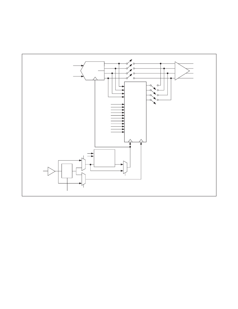
�Figure� 3.� DSP� Interface� Top-Level� Connectivity� and� Control� Signals�
�ter.� This� selects� between� bit� 0� ;� bit� 0� and� bit� 1� ;� bit� 0� and� bit� 2� ;�
�and� bit� 0� ,� bit� 1� ,� bit� 2� ,� and� bit� 3� cases.� If� only� bit� 0� is� serial-�
�ized,� the� data� stream� consists� of� bit� 0� data� only.� If� a� seri-�
�alization� of� bit� 0� and� bit� 1� (or� bit� 2� )� is� selected,� the� stream�
�data� pattern� consists� of� 16� bits� of� bit� 0� data� followed� by�
�16� bits� of� bit� 1� (or� bit� 2� )� data,� which,� in� turn,� is� followed� by�
�16� bits� of� bit� 0� data,� and� so� on.� In� this� case,� the� serial�
�clock� must� be� at� least� twice� as� fast� as� the� ADC� clock.� If� a�
�4-bit� serialization� of� bit� 0� ,� bit� 1� ,� bit� 2� ,� and� bit� 3� is� chosen,� the�
�serial� clock� must� be� at� least� four� times� faster� than� the�
�ADC� clock.�
�The� ADC� data� is� loaded� in� parallel� into� four� holding� reg-�
�isters� that� correspond� to� four� ADC� outputs.� Holding� reg-�
�isters� are� 16� bits� long� and� are� clocked� by� the� ADC� clock.�
�14�
�At� the� end� of� the� 16-bit� ADC� cycle,� the� data� is� trans-�
�ferred� into� four� shift� registers� and� shifted� serially� to� the�
�output� during� the� next� 16-bit� ADC� cycle.� Shift� registers�
�are� clocked� by� a� serial� clock� that� must� be� chosen� fast�
�enough� so� that� all� data� is� shifted� out� before� the� next� set�
�of� data� is� loaded� from� the� ADC.� An� all-zero� pattern� fol-�
�lows� the� data� after� all� valid� ADC� data� are� streamed� to� the�
�output.� A� DATASYNC� signal� is� used� to� signal� the� begin-�
�ning� of� each� valid� 16-bit� data� slice.� In� addition,� there� is� a�
�TIME_SYNC� signal� that� is� output� every� 128� to� 16,384�
�cycles� of� the� ADC� clock.�
�Maxim� Integrated�
�发布紧急采购,3分钟左右您将得到回复。
相关PDF资料
MAX2821ETM+T
IC TXRX 802.11B 2.4GHZ 48-TQFN
MAX2829EVKIT
EVAL KIT MAX2828, MAX2829
MAX2830EVKIT+
KIT EVAL FOR MAX2830
MAX2831EVKIT+
KIT EVAL FOR MAX2831
MAX2837EVKIT+
KIT EVAL FOR MAX2837
MAX2838EVKIT+
KIT EVAL FOR MAX2838
MAX2839ASEVKIT+
KIT EVAL FOR MAX2839A WLP
MAX2839EVKIT+
KIT EVAL FOR MAX2839
相关代理商/技术参数
MAX-277
制造商:MDE 制造商全称:MDE Semiconductor, Inc. 功能描述:HIGH CURRENT TRANSIENT VOLTAGE SUPPRESSOR
MAX280C/D
功能描述:有源滤波器 RoHS:否 制造商:Maxim Integrated 通道数量:1 截止频率:150 KHz 电源电压-最大:11 V 电源电压-最小:4.74 V 最大工作温度:+ 85 C 安装风格:Through Hole 封装 / 箱体:PDIP N 封装:Tube
MAX280CPA
功能描述:有源滤波器 RoHS:否 制造商:Maxim Integrated 通道数量:1 截止频率:150 KHz 电源电压-最大:11 V 电源电压-最小:4.74 V 最大工作温度:+ 85 C 安装风格:Through Hole 封装 / 箱体:PDIP N 封装:Tube
MAX280CPA+
功能描述:有源滤波器 5th-Order Zero-Error Butterworth RoHS:否 制造商:Maxim Integrated 通道数量:1 截止频率:150 KHz 电源电压-最大:11 V 电源电压-最小:4.74 V 最大工作温度:+ 85 C 安装风格:Through Hole 封装 / 箱体:PDIP N 封装:Tube
MAX280CWE
功能描述:有源滤波器 Integrated Circuits (ICs) RoHS:否 制造商:Maxim Integrated 通道数量:1 截止频率:150 KHz 电源电压-最大:11 V 电源电压-最小:4.74 V 最大工作温度:+ 85 C 安装风格:Through Hole 封装 / 箱体:PDIP N 封装:Tube
MAX280CWE+
功能描述:有源滤波器 5th-Order Zero-Error Butterworth RoHS:否 制造商:Maxim Integrated 通道数量:1 截止频率:150 KHz 电源电压-最大:11 V 电源电压-最小:4.74 V 最大工作温度:+ 85 C 安装风格:Through Hole 封装 / 箱体:PDIP N 封装:Tube
MAX280CWE+T
功能描述:有源滤波器 5th-Order Zero-Error Butterworth RoHS:否 制造商:Maxim Integrated 通道数量:1 截止频率:150 KHz 电源电压-最大:11 V 电源电压-最小:4.74 V 最大工作温度:+ 85 C 安装风格:Through Hole 封装 / 箱体:PDIP N 封装:Tube
MAX280CWE-T
功能描述:有源滤波器 RoHS:否 制造商:Maxim Integrated 通道数量:1 截止频率:150 KHz 电源电压-最大:11 V 电源电压-最小:4.74 V 最大工作温度:+ 85 C 安装风格:Through Hole 封装 / 箱体:PDIP N 封装:Tube